I have a dilemma. How should I implement the H bridge?
Each has their own advantages and disadvantages. One choice is the use of the MOSFET over the BJT. I have chosen the MOSFET because it has zero current going through its gate, while the BJT current can be significant, contributing to complications.
I want a small voltage across the device when it has maximum current. In this region of operation, the BJT causes charge to build up. This charge takes time to dissipate. The MOSFET is much faster in this region of operation. Also, the minimum voltage for the BJT is much higher, and is independent of the base voltage. The minimum voltage for the MOSFET for a given current is much lower, and it does depend on the gate to source voltage. The equation for the MOSFET is much simpler to implement, and is readily adapted to many specifications. The transport model for the BJT has many more variables and equations, that could be beneficial when looking for a solution.
One final consideration is whether to use complementary p and n MOSFET transistors, or if I should only use n MOSFET transistors.
Using complementary transistors has some advantages, but they might also turn into disadvantages. A major disadvantage is each pair of kitty corner transistors now must have opposite highs and lows. Both types must change the voltage from digital 5 Volts to a voltage more suitable to turn the transistor on. Unless the gate voltage must be much higher than the voltage required to drive the desired current through the load, the highest voltage needed would be the power supply voltage.
If we chose to use 4 n MOSFETs, turning each transistor off would be made much simpler, since 0 Volts will do that. Turning the two upper, current source, transistors on would be more difficult, because now the gate voltage must be much higher than the voltage across the load.
This is only the tip of the ice berg. I am sure more challenges lay ahead.
http://www.linkedin.com/in/andrewvall
http://www.elance.com/provprofile?userid=184021&rid=3QOZ
Electrical Design Engineer, Minneapolis, Minnesota
Monday, December 20, 2010
Saturday, December 18, 2010
MOSFET Power Amplifier
In circuit design, power efficiency is a tricky business. The key is to put all of the power originating from the power supply to the load. The trouble is, active circuits do not do that very well over their whole range. Ideally, you want the power dissipated from the transistor to be zero for most of the time. Power is current times voltage. The most efficient amplifier have zero current at maximum voltage, and zero voltage at maximum current. This is the essence of why using a Class D power amplifier or an H bridge is such a good idea. Except, the amplifier is only as good as its components.
The specifications for this design are as follows. It is to have only one power supply, 5 Volts, and a ground. This means that 5 Volts at the gate of the n channel enhancement mode MOSFET should turn the transistor on all the way, and 0 Volts should turn the p channel enhancement mode MOSFET all the way. The MOSFET should have zero volts across from drain to source, when it has been turned on.
The current needed through the amplifier depends on the current through the load. For instance, a speaker usually has an internal resistance of 8 Ohms. Most speakers are rated at a given power level, like 100 Watts.
 The current through the load is the square root of the watts divided by the resistance. The current a 100 Watt 8 Ohm speaker is rated for is 3.5 Amps. The resulting voltage across the load is 28 V. Thus, I have misspoken. The voltage level must be boosted to over 28 Volts to drive the load at 3.5 Amps. Thus, the gate voltage for the p channel MOSFET must also be boosted to 28 Volts, or else the voltage from the gate to source will never be equal to zero.
 This is the operation of the circuit. Transistor 11 and 12 must never be on at the same time. Same holds true for 21 and 22. The load gets current if 11 and 22 are both on, or 12 and 21 are both on. The current directions for each are opposite of each other. Voltage source 1 and 3 are opposites of each other. Same with Voltage source 2 and 4. They can be driven by the same PWM signal, just so one is high while the other is low.
The next task is to find a way to get 3.5 Amps through the transistors. Since the linear or triode region of operation is the most interest to me, I should start there.


Because I know the current, the gate source voltage, the approximate drain source voltage, and many of the other parameters I want, I can solve for the width to length ratio start designing the other components for the power dissipation. Unfortunately, discrete devices are not so easily designed for. I must pick from an assortment of discrete devices, each with their own advantages. The most important parameter for all of these components is their ability to hold 3.5 Amps of current. Using a site like Digikey streamlines the process of narrowing down a selection, but the task is still daunting. That is the next step in the process.
Microelectronic Circuit Design, Richard Jaeger
http://en.wikipedia.org/wiki/Watt
http://www.linkedin.com/in/andrewvall
http://www.elance.com/provprofile?userid=184021&rid=3QOZ
Electrical Design Engineer, Minneapolis, Minnesota
The specifications for this design are as follows. It is to have only one power supply, 5 Volts, and a ground. This means that 5 Volts at the gate of the n channel enhancement mode MOSFET should turn the transistor on all the way, and 0 Volts should turn the p channel enhancement mode MOSFET all the way. The MOSFET should have zero volts across from drain to source, when it has been turned on.
The current needed through the amplifier depends on the current through the load. For instance, a speaker usually has an internal resistance of 8 Ohms. Most speakers are rated at a given power level, like 100 Watts.

The next task is to find a way to get 3.5 Amps through the transistors. Since the linear or triode region of operation is the most interest to me, I should start there.
For n channel enhancement mode MOSFET
For p channel enhancement mode MOSFET
So, there lies the problem. The smaller the drain source voltage is, the smaller the drain current. The electron mobility and the oxide capacitance are essentially the same for most silicon devices The electron mobility depends on temperature and impurity concentrations. The electron mobility is 40% less for p channel devices. The largest contributing factor is the width to length ratio.Because I know the current, the gate source voltage, the approximate drain source voltage, and many of the other parameters I want, I can solve for the width to length ratio start designing the other components for the power dissipation. Unfortunately, discrete devices are not so easily designed for. I must pick from an assortment of discrete devices, each with their own advantages. The most important parameter for all of these components is their ability to hold 3.5 Amps of current. Using a site like Digikey streamlines the process of narrowing down a selection, but the task is still daunting. That is the next step in the process.
Microelectronic Circuit Design, Richard Jaeger
http://en.wikipedia.org/wiki/Watt
http://www.linkedin.com/in/andrewvall
http://www.elance.com/provprofile?userid=184021&rid=3QOZ
Electrical Design Engineer, Minneapolis, Minnesota
Thursday, December 16, 2010
LED and resistor
There are many different options for controlling an LED. If the current is small, and the power dissipated not very great, a simple resistor would suffice.
A resistance in series with the LED will limit the current through it. One must make sure there is adequate voltage across the LED to it on. A quick look at the data sheet can tell a person a voltage and a current to go along with that voltage, using the voltage current characteristics graph. Then all they have to do is subtract that voltage from the power supply, and find the resistance value that will allow that specified current through for that amount of voltage.
http://www.linkedin.com/in/andrewvall
http://www.elance.com/provprofile?userid=184021&rid=3QOZ
Electrical Design Engineer, Minneapolis, Minnesota
Saturday, December 4, 2010
Low Pass Filter for an H-Bridge
Analog signals are easily corrupted. Unless the line they are on is relatively short, their fidelity will be compromised, and the signal will be lost. This is most apparent for sound signals to speakers. Professional engineers spend years fine tuning the system, so noise will be kept at a minimum. Amateur systems keep all of the components close together and lines relatively short, so that noise will not be an issue. What if you want to place speakers clear on the other side of a room? No analog solution exists, or is prohibitively expensive.
A digital solution might exist, granted that it is fast enough. Some more information on what that solution might entail exists here. It consists of either a class D amplifier or an H bridge, driven by PWM, and using a carrier signal. To filter out the carrier signal after the class D amplifier requires either an RC, RLC, or active filter. The problem with all of the class D amplifier is it requires the use of two power supplies.
The H bridge doesn't require two power supplies, but the choice of filters is much more limited. Here is one implementation.
 It has two inductors, in series with the load (resistor), and a capacitor in parallel with the load. Here is a close up of the filter.
 The resistance and capacitance form an impedance, and all the currents are equal.

The currents, being equal, is just the voltage across the filter divided by the impedance.
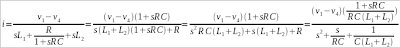
The voltage of interest is that across the resistance.

What results is a second order low pass filter, where omega not is the cut off frequency, and Q is the amplitude at that frequency. To obtain a maximally flat response, Q must equal the square root of one over two. The cut off frequency is this.

Q is this.

Leading to this.
 Again, as with the other passive filters, to obtain a small cut off frequency, the inductor and capacitor will have to be very large. The carrier signal will have to be as large as possible, to keep the components economical and small. Clearly, this is no small engineering feat.
http://www.linkedin.com/in/andrewvall
http://www.elance.com/provprofile?userid=184021&rid=3QOZ
Electrical Design Engineer, Minneapolis, Minnesota
A digital solution might exist, granted that it is fast enough. Some more information on what that solution might entail exists here. It consists of either a class D amplifier or an H bridge, driven by PWM, and using a carrier signal. To filter out the carrier signal after the class D amplifier requires either an RC, RLC, or active filter. The problem with all of the class D amplifier is it requires the use of two power supplies.
The H bridge doesn't require two power supplies, but the choice of filters is much more limited. Here is one implementation.


The currents, being equal, is just the voltage across the filter divided by the impedance.
The voltage of interest is that across the resistance.

What results is a second order low pass filter, where omega not is the cut off frequency, and Q is the amplitude at that frequency. To obtain a maximally flat response, Q must equal the square root of one over two. The cut off frequency is this.
Q is this.
Leading to this.
http://www.linkedin.com/in/andrewvall
http://www.elance.com/provprofile?userid=184021&rid=3QOZ
Electrical Design Engineer, Minneapolis, Minnesota
Subscribe to:
Comments (Atom)